
PCB Layout Engineering
Serving the Electronics industry since 1979
Additional Capabilities
Flexible Support for you Project
Whether you need complete PCB development or additional layout capacity, GS Designs provides experienced, flexible support tailored to your requirements. We work closely with your engineering team, offering both off and on site availability to suit your project..


Email:peter@gsdesign.co.uk Telephone +447809203494
Schematic Capture
Clear, well-documented Designs
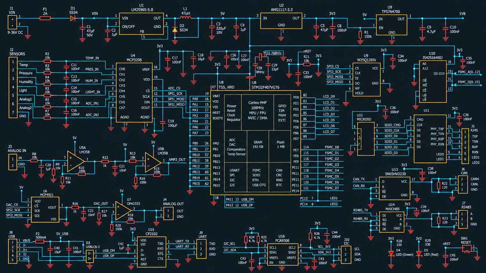
professional electronic schematic development using Altium Designer, clear organised and fully documented designs to support efficient project delivery
Schematic capture — clear, structured schematics created in Altium Designer.
Multi-sheet designs — logical organisation of complex circuits across multiple sheets..
Hierarchical schematics — functional blocks that make larger designs easier to navigate
Component libraries — management of schematic symbols and PCB footprints.
Component data — manufacturer part numbers, values and supporting information.
Bill of materials — structured component lists to support purchasing and assembly.
Legacy schematic conversion — recreation of designs from PDFs, drawings and older CAD formats
PCB Layout and design
Complex Designs. Practical Solutions
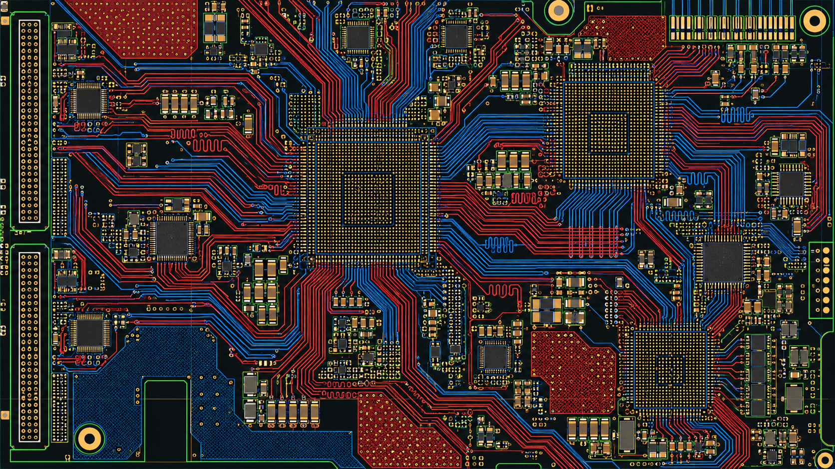
Expert PCB layout, from straightforward boards to complex, high-performance designs. We share progress at every critical stage, keeping your team informed and fully involved throughout the design process.
DDR memory routing — matched-length routing for DDR interfaces.
Controlled impedance — single-ended and differential routing to suit the board stack-up.
Differential pair routing — precise pair spacing, coupling and length matching.
High-speed interfaces — layout for PCIe, USB, Ethernet, HDMI and LVDS.
Microvia and HDI design — fine-pitch component using microvias, blind and buried vias.
Layer stack-up planning — signal and plane arrangements for high-speed performance.
Return path management — maintaining continuous reference planes.
Manufacturing Support
Ready for Production
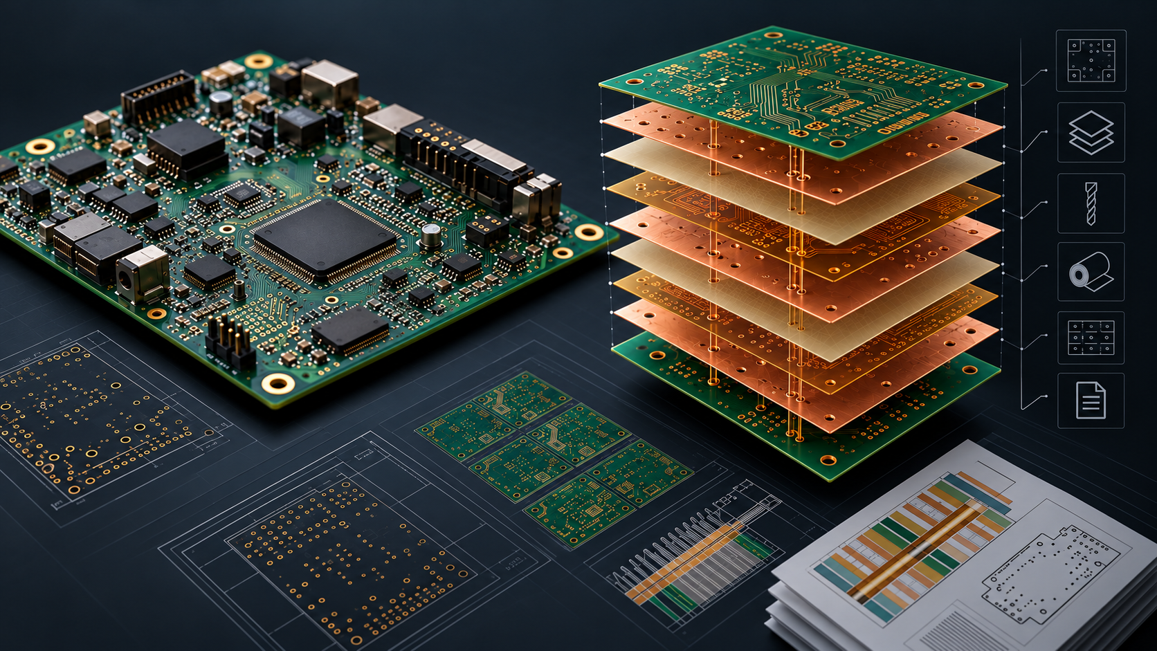
Comprehensive manufacturing data packages to ensure a smooth transition from design to production.
Gerber files — fabrication data for copper layers, solder mask and silkscreen.
ODB++ data — manufacturing data for PCB fabrication and assembly.
NC drill files — drilling data for plated and non-plated holes
Fabrication drawings — dimensions, tolerances and manufacturing notes..
Impedance requirements — controlled impedance targets
Pick-and-place files — component positions and rotations for automated assembly.
3D STEP models — board and component models for mechanical integration.
Design Tools
Altium Designer Specialist
GS Designs use Altium 365 as its primary design tool, drawing on over 20 years of experience with the platform. Our detailed knowledge of its integrated schematic capture, PCB layout and library management tools supports an efficient and consistent design process. Altium 365 supports collaboration, design reviews and revision management, keeping your team involved from initial capture through to final release.