
PCB Layout Engineering
Serving the Electronics industry since 1979


Email Peter@gsdesign.co.uk Telephone : +44 7809203494
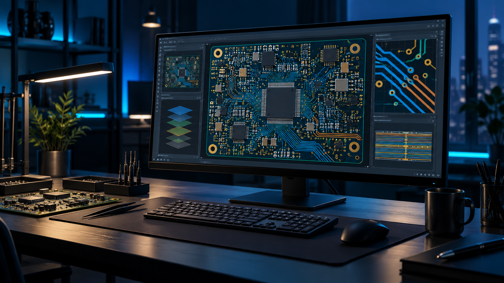
PCB Layout
Component placement, routing and complete PCB layout development for simple to complex, high performance designs
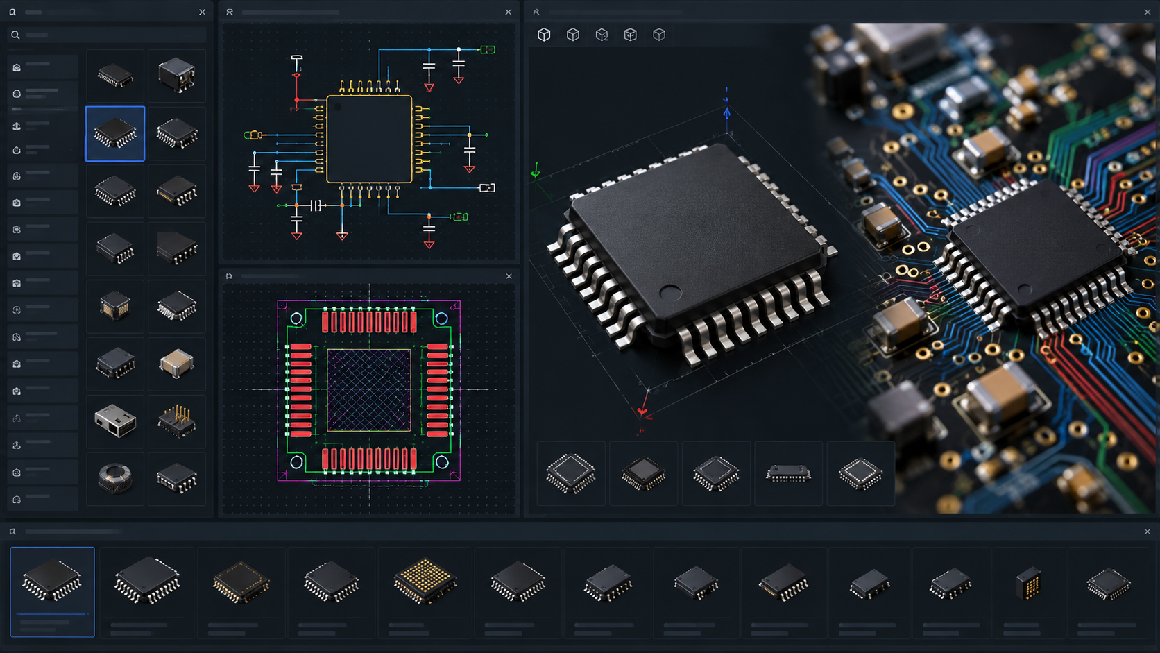
PCB Library management
Creation, maintenance and validation of Schematic symbols. PCB footprints and component libraries to ensure consistency and reliability.
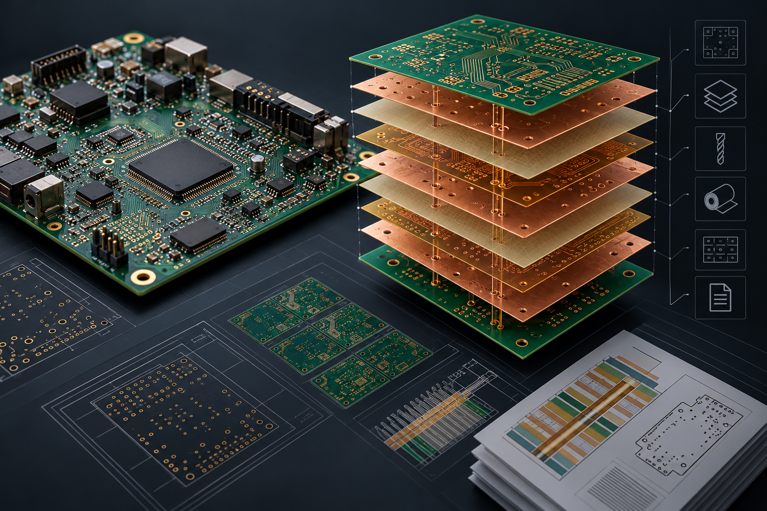
Manufacturing Data
Production-ready data to ensure a smooth transition from design to manufacture, including fabrication files, assembly drawings and supporting documentation
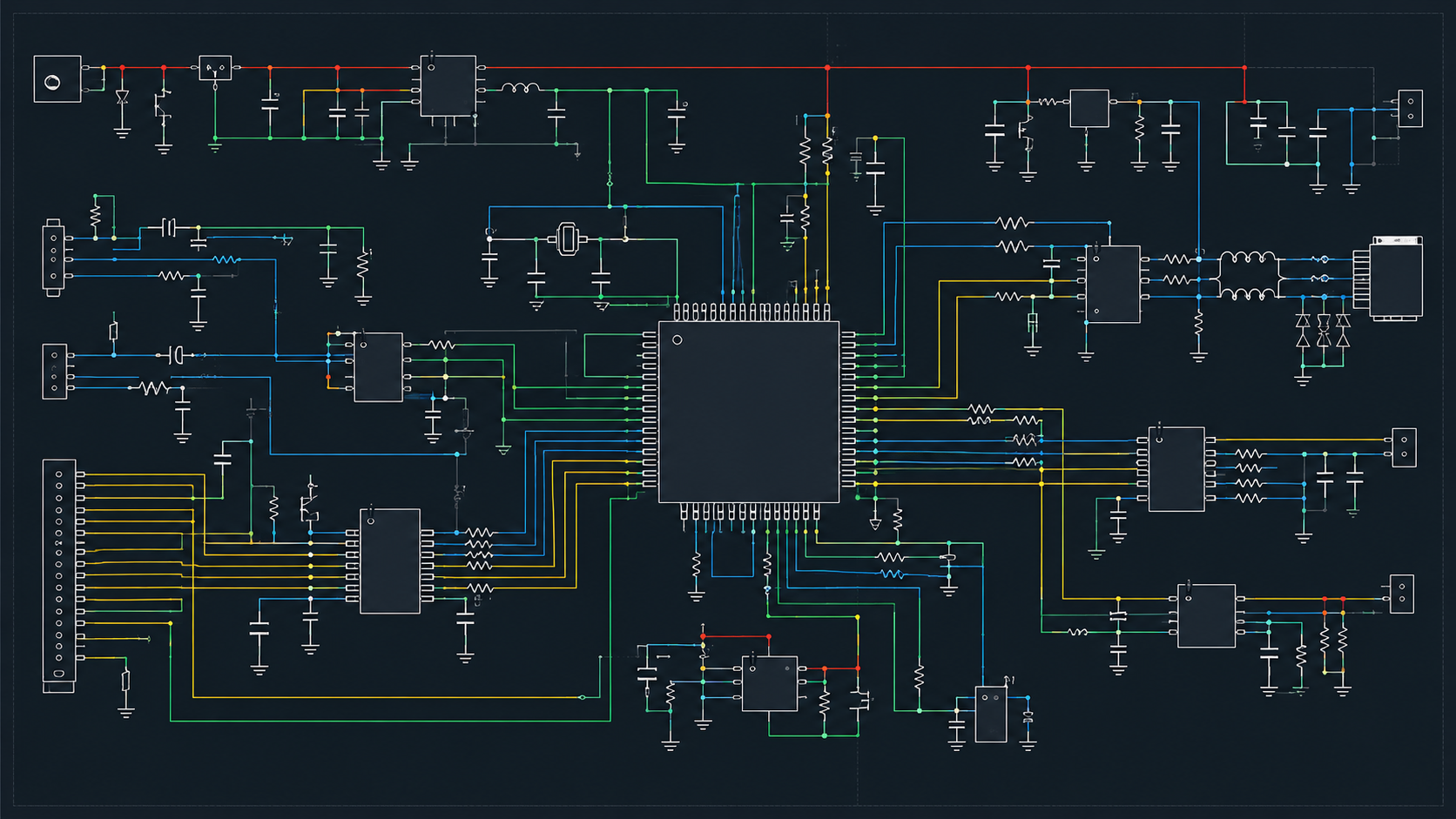
Schematic Capture
Schematic development using Altium 365, Clear, well-structured and fully documented designs
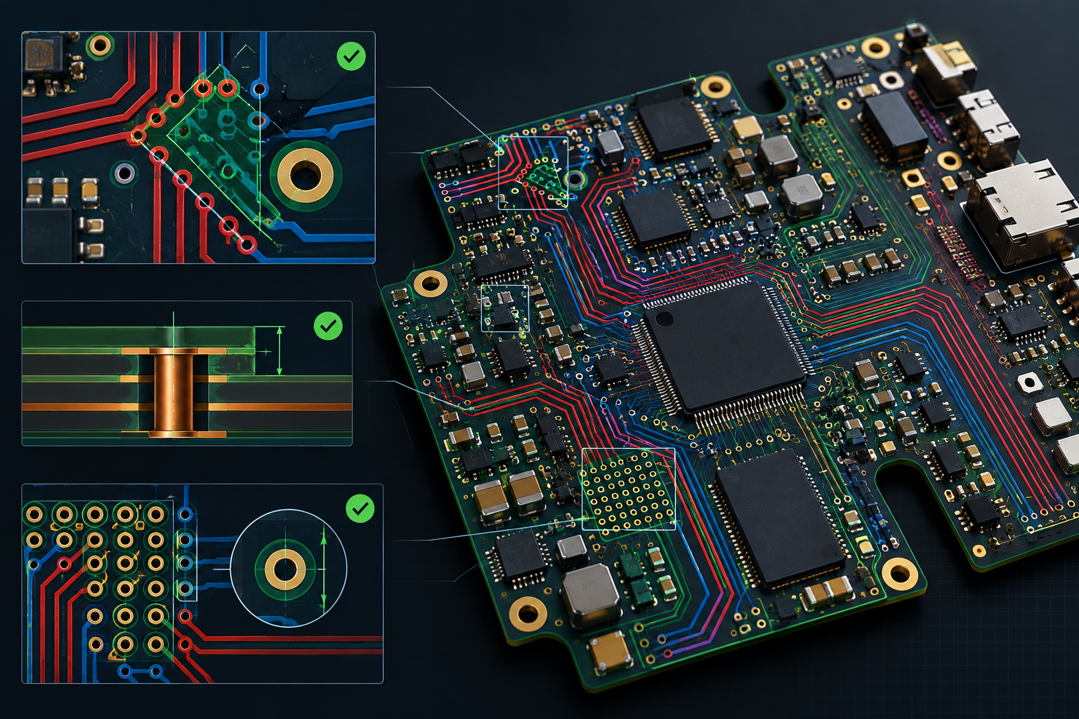
Design Verification & DFM
Design reviews, rule checking and design for manufacture assessments to optimise performance and manufacturability.
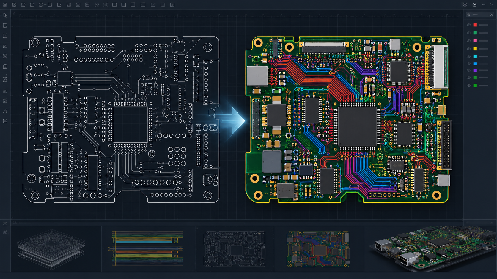
Design Updates & Legacy CAD Conversion
Modification, updating and redevelopment of existing PCB designs, including legacy projects